
As you probably know, one of Digilent’s major focuses is producing FPGA (field programmable gate array) boards and educating the public on FPGA design. One of the classes I was in last semester focused on FGPA design. This class is EE324 at WSU, which is taught by Digilent’s own Clint Cole. He gave a background lecture on the History of FPGA chips. Not only was it an extremely interesting lecture, but it also helped me understand the huge leaps in logic design that have been made since the 1960s. This is the history that led to the development of FPGA chips. The chips are the parts that Xilinx makes that we use on our FPGA boards.
I’ve compiled a brief timeline of some of the inventions that have lead to FPGA technology. In the FPGA community, there is quite a bit of contention over who invented what first, so I’ve decided to focus my timeline on what the invention was and how it led to the invention of the FPGA. There is some uncertainty about the dates when a few of the devices were invented, so I picked the dates that occurred most frequently.
A Brief Timeline of the Steps Leading to FPGA Development:
1960 — First MOSFET
MOSFETs (metal–oxide–semiconductor field-effect transistor) are one of the most basic elements in an FPGA. In the world of FPGAs, they are usually referred to as gates. They are used similar to switches. Depending on what value they recieve, 0 or 1, they will either block or allow the flow of current. There are two main types of MOSFETs, PFETS and NFETS.
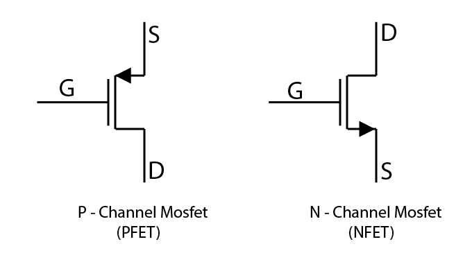
NFETs turn on, allow current, and when past a 1, PFETS act in the opposite way. When you program the FPGA chip, it has to arrange all these MOSFETs so they provide the required output. One example of how they work is in a NAND gate. A NAND gate performs the not-AND operation. Below is the circuit diagram for a NAND gate using PFETs and NFETs.
Nand Circuit
Image from Wikipedia.
https://en.wikipedia.org/wiki/CMOS#/media/File:CMOS_NAND.svg
Sometimes, NFETS and PFETs are shown without the arrows but with a circle on the gate to denote a PFET. In the image, you can see that if A and B are past a 0, the two PFETs on the top will be turned on and the two NFETs connected to Vss or ground will be off, so VDD will be passed, or logically it will pass a 1. Since the PFETs are in parallel, if at A or B are 0, Vdd will be passed and ground will be disconnected. So this acts as a NAND gate should, 0 will only be passed if ground is connected. Ground is connected only if both A and B are 1 and the NFETs are turned on.
For more in-depth information on MOSFETs, click here.
1961 — First Communication IC
An IC (integrated circuit) is a small chip that has a set circuit on it. For example, you can buy an IC that just has a mux on it. ICs were an upgrade from using transistors to build circuits, because they are generally printed. This way you can print an entire circuit in one shot, rather than having to assemble the circuit with possibly thousands of transistors. This saves time and space.
When you write an FPGA project in HDL (hardware design language), you instantiate modules in code. This would be analogous to ordering ICs of each of the modules that you need and physically wiring them together. Of course then you don’t have the protection that FPGA chips offer, and it’s very easy to burn out your ICs. ICs were one of the major building blocks in FPGAs for this reason. Engineers had a way to “customize” circuits by putting together multiple ICs, but this process was long and painful and not as automated as coding the blocks. On top of that, they aren’t as reusable. You can’t simply reprogram your circuit like you can an FPGA. Another problem with ICs is that your circuits very quickly become huge.
However, ICs aren’t irrelevant. In fact there are quite a few in the chipKIT Starter Kit, such as the mux IC. An example of how this is used can be found in this project.
For more information in ICs, click here.
1962 — First TTL
TTL (transistor-transistor logic) is a family of ICs. Rather than being made of MOSFETs like the ICs, a TTL is made with BJTs (bipolar junction transistors). The main advantage of the TTL over the IC is that it consumes less power and is less sensitive to damage from electrostatic discharge.
For more information on TTL, click here.
1963 — First CMOS
A CMOS (complementary metal-oxide semiconductor) is again an improvement on the IC technology, but this time an improvement on how they are constructed. The PFETs and NFETs in CMOS circuits are paired so that one in each pair is always off. This reduces waste heat as there is no standing current during transition.
For more information on the CMOS, click here.
1965 — Moore’s Law
In 1965, Moore’s Law was delineated. This law is based on the prediction that the number of transistors in a circuit doubles every year. This law is now used in industry and research to set goals. Unfortunately, soon Moore’s Law may not hold, as technology is getting to the point where transistors are a number of silicon atoms wide. If you would like to read more about the limiting size of transistors and the end of Moore’s Law, Purdue produced an article about it in 2012.
For more information on Moore’s Law, click here.
1970 — PROM
PROM (programmable read-only memory) was one of the first types of programmable memory. Previously there had been ROM (read-only memory) where the data was set at manufacturing. Although PROM was a huge step in programmable technology, there was still improvement to be made, as it wasn’t re-programmable. Once you set the memory, it was permanent.
For more information on PROM, click here.
1971 — EPROM
EPROM (erasable programmable read-only memory) was the second step in programmable memory, in that you could erase it. To erase an EPROM, you had to shine UV-light directly on the EProm. However, this type of erasing isn’t the most practical, as you would have to take the EPROM out of the circuit to erase it.
For more information on EPROM, click here.
1972 — DST
A DST (depleted-substrate transistor) is similar to a MOSFET, except that it has no voltage difference from its gate to source. This provides higher gain and low noise as compared to a normal MOSFET.
For more information on the DST, click here.
1975 — PLA
A PLA (programmable logic array) is made up of programmable AND gate planes and programmable or gate planes, connected to product a desired output. With this type of programmable logic you could most directly implement POS (product of sums), or gates then and gates, and SOP(sum of products), and gates then or gates, which are now only used as a formalism in design, and teaching tool. This allowed for programmable logic, but nothing near the complexity of design that FPGAs allow.
For more information on the PLA, click here.
1978 — PAL
PAL (programmable array logic) is similar to PLA; however, rather than having two programmable planes, it instead has one PROM array, a fixed OR plane and a programmable AND plane. This only allows for sum of products logic equations with feedback from the outputs.
For more information on PAL, click here.
1983 — EEPROM
EEPROM (electrically erasable programmable read-only memory) offered a huge improvement from EPROM, in that you didn’t have to shine UV light on the memory to erase it. It was memory that was finally erasable electrically. This allowed for data to be read, erased, and reprogrammed. However, EEPROMs only allow for a certain number of times it can be reprogrammed.
For more information on EEPROM, click here.
1983 — GAL
GAL (generic array logic) was a major improvement on PAL. GAL is completely erasable and re-programmable.
For more information on GAL, click here.
1984 — FLASH
Flash memory is a type of EEPROM, and it is the most commonly used non-volatile memory. One major improvement from the EEPROM is that FLASH memory can be erased in blocks. So, rather than having to erase all of the memory and rewrite it, you can choose what memory to erase.
For more information on FLASH, click here.
1985 — First FPGA
And finally in 1985, the first FPGA was developed!
For more information on FPGA, click here.
Stay tuned into the blog for a post on the structure of the FPGA!
Very well written!
I will right away snatch your rss feed as I can not find your
e-mail subscription hyperlink or e-newsletter service.
Do you’ve any? Please allow me know so that I may just subscribe.
In fact Xilinx does not create the term FPGA, they called their XC2064 a LCA device (Logic Cell Array). The term FPGA was coined by Actel, I suppose.
Should CPLD be included in this list, such as Digilent used to sell? Ref https://digilent.com/shop/coolrunner-ii-cpld-starter-board-limited-time/