
Earlier you read about logic gates and their functions. Then you read about how to code logic gates in Verilog, VHDL, and C. Now its time to learn about creating logic gates with transistors. After reading all of these posts you will have learned about logic gate theory, coding logic gates in both hardware and software, and the physical hardware design of logic gates.
The first thing to know before we get into the structure of logic gates is the two types of transistors that will be used. There are NFETs (n-type or n-channel mosfet) and PFETs (p-type or p-channel mosfet.)
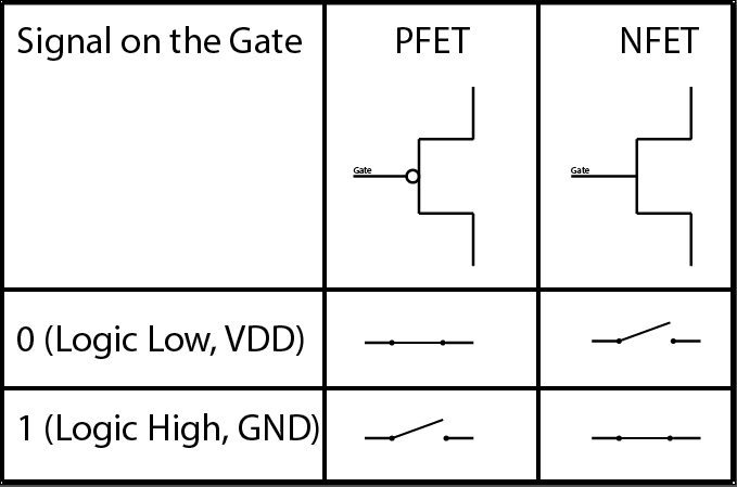
PFETs are like switches that are closed when the gate is given a 0 and are open when the gate is given a 1. In other words, a PFET will pass a value through it when it receives a 0.
NFETs are like switches that are closed when the gate is given a 1 and are open when the gate is given a 0. In other words, a NFET will pass a value through it when it receives a 1.
To make our logic gates we can use a combination of NFETs and PFETs.
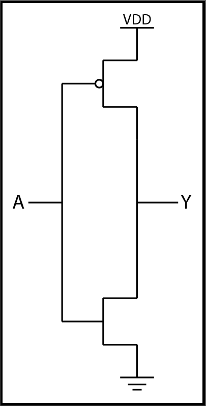
The NOT gate only uses two transistors. If A is 1, then the PFET is off and the NFET is on, so GND or 0 gets passed. If A is 0 the PFET is on and the NFET in off so VDD or 1 gets passed.
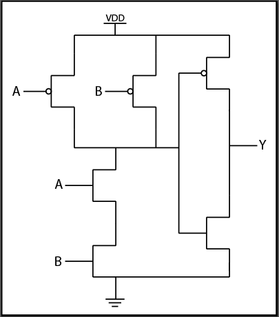
The AND gate is slightly more complicated and requires six transistors. You can still go through the same process as before to see how it works. Give A and B values and see which transistors are on, and what values get passed.
The NAND gate is very closely related to the AND gate. Notice that the NAND gate is an AND gate without the NOT gate at the end.
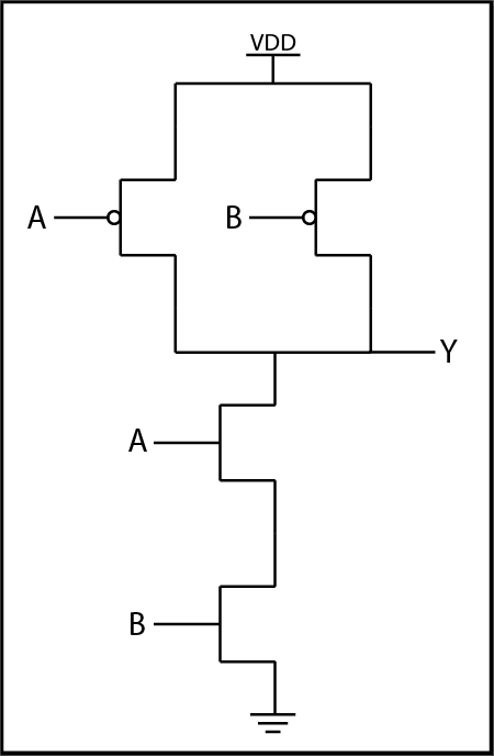
The OR gate is very similar to the AND gate, except that the NFETs are in parallel rather than the PFETs being in parallel.

The NOR gate has the same relationship with the OR gate that the NAND gate has with the AND gate.
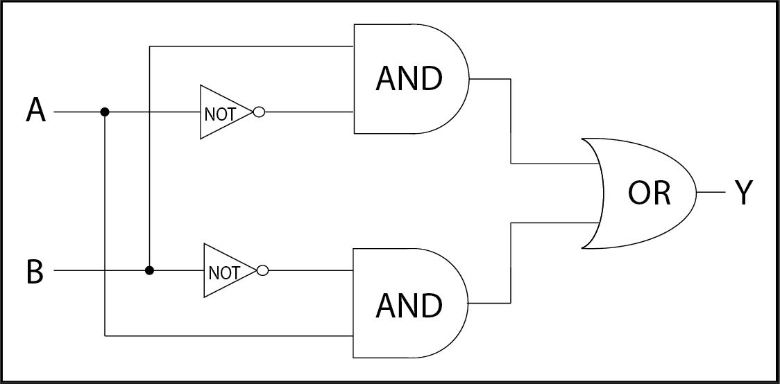
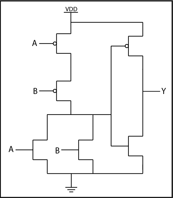
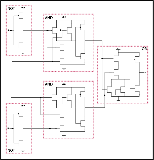
The XOR is quite a bit more complicated. It can be made up of five of the gates that we already described. You can see the block diagram describing how these gates are combined. In the transistor image I enclosed each gate in red dots.
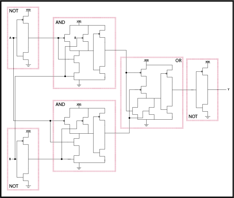
The XNOR gate has the same relationship with the XOR gate that NAND has with AND and that NOR has with OR. Notice that in the XNOR gate the last NOT gate and the NOT gate in the OR gate can be cancelled out. Two negatives, in this case, do make a positive. So instead of the OR and NOT you could just use a NOR gate.
Now that you have an understanding of the basic logic gates used in digital design, check out the FPGA modules on Digilent’s Learn site!
Are you ready to unleash your creativity and dive into the world of digital design? Explore the endless possibilities with Digilent FPGA boards and bring your ideas to life!
Thanks