
Once upon a time, the readers of the Digilent blog were given a brief history lesson on the field programmable gate array (FPGA), at the end of which you all were promised a follow up on the structure of the FPGA. As time passed, that commitment slipped from memory and was nearly fully forgotten. If you have heeded the call to ‘Stay tuned’ since that original post, then your patience is about to be rewarded with a series covering the inner workings of the FPGA. We begin in this post with a brief summary of the some things, and some stuff, based on an analysis of the Xilinx 7-series FPGAs (Basys 3, Nexys A7, Cmod A7, Arty S7, Arty A7, and Cmod S7 are examples. All can be found on our FPGA product page).
Modern FPGAs contain components that are specialized for specific functions as well as more general purpose configurable logic. The combination of dedicated functionality components with the configurable logic has allowed for architectures that consume less power and perform more efficiently.
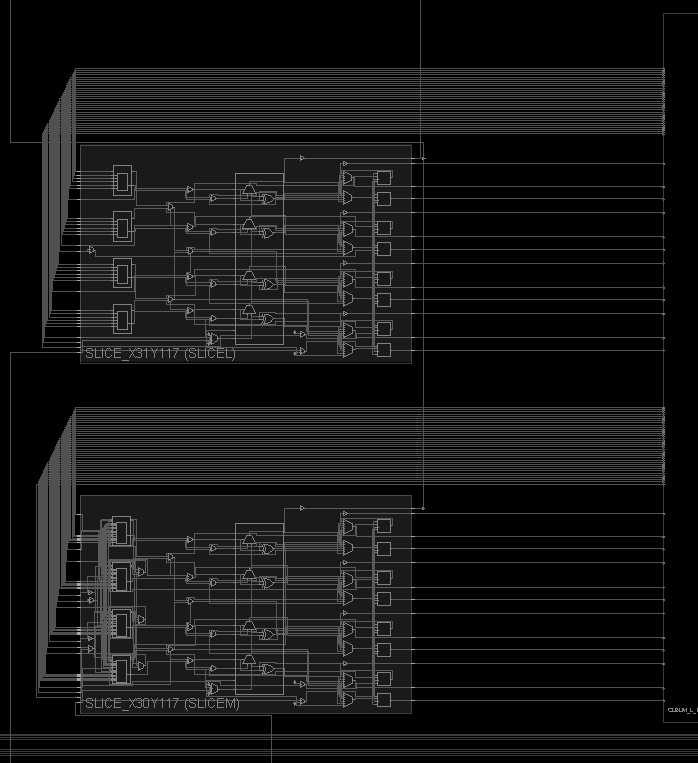
Configurable Logic Block (CLB)
A CLB is the fundamental piece of an FPGA and is what gives it its ability to take on different hardware configurations. An FPGA in its most basic form is a chip of CLBs–together, they make an FPGA. The many thousands of these that can be found on modern FPGAs can be programmed to perform virtually any logic function. An individual CLB consists of a number of discrete logic components itself, such as look-up tables (LUTs) and flip-flops.
Digital Signal Processing (DSP) Slice
Referred to as a DSP slice, block, or cell, this is one of the specialized components in an FPGA. It is designed to carry out digital signal processing functions, such as filtering or multiplying, much more efficiently than if the same functions were implemented using many CLBs.
Transceivers
The name of this component is a mash up of its functionality, as they are made to transmit and receive serial data (individual bits) to and from the FPGA at extremely high rates. The task of converting information on the FPGA into serial data, as well as receiving serial data externally and converting it into useful information, while checking for errors in the data becomes more difficult to do with the configurable logic of the FPGA as speeds increase, eventually hitting a speed cap. Having a dedicated component available for this allows for easy implementation of high speed data transfer by the user without consuming the logic resources of the FPGA.
Block Random Access Memory (BRAM)
Memory available on an FPGA board comes in a few flavors, however the dedicated memory on the chip itself is referred to as block RAM or BRAM. While each block individually is of a set size (36K bits for Xilinx 7 series chips), these blocks can be subdivided or cascaded to make smaller or larger sizes of BRAM available. They also are capable of a variety of operational settings and can support special functionality such as error correction
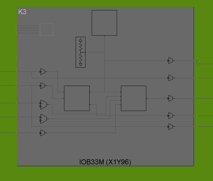
Input/Output (IO) Blocks
Input/output blocks are pretty much what they sound like. They are the components through which data transfers in to and out of the FPGA. Input and output on the chip goes through component groups called IO banks, which consist of 50 individual IO blocks. The IO blocks themselves are configurable in a number of ways depending on the type of data the user is either expecting to receive or transmit. These are similar to transceivers but operate at lower speeds and can maintain more functional flexibility. A simple analogy to distinguish the two would be to consider having a choice of vehicle between a car (IO block) and a jet (transceiver) for a commute. Even if the distance allowed you could get up to speed to take off in the jet (transceivers have minimum operating speeds), it would be wildly impractical.
Each of these components contains its own subset of discrete parts and unique architecture that enable it to function. The details pertaining to each are beyond the scope of this post, however, the follow ups in this series will explore the inner working of each in greater detail, so stay tuned!